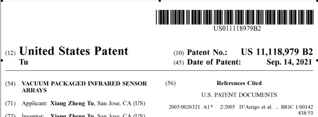
Develop a Vacuum Packaged Infrared Imaging Sensor Array
Utilizing
Xiang Zheng Tu
A major advantage of infrared imaging sensors is their ability to detect living objects. They operate effectively in both day and night conditions and provide all-weather capability.
Wafer-Level Vacuum Packaging Process
The sensors are produced on a semiconductor wafer using materials such as silicon, indium antimonide, or mercury cadmium telluride, tailored to the application and required wavelength range.
Micro-Electromechanical Systems (MEMS) Integration**: Integration of MEMS technology with the sensors on the same wafer often includes micro-optical components like lenses and mirrors, as well as mechanical components such as actuators.
Following fabrication, the wafer is encapsulated to create a vacuum seal. This usually involves bonding a cap wafer or a glass lid to the sensor wafer using methods like anodic bonding, fusion bonding, or adhesives compatible with the operational environment.
The encapsulation process is followed by dicing the wafer into discrete units, each containing one sensor package.
Advantages of Wafer-Level Vacuum Packaging
This technique produces extremely compact sensor packages, ideal for space-constrained applications such as in mobile devices or compact electronics.
Simultaneous packaging of multiple sensors on a wafer scale significantly reduces manufacturing costs compared to packaging sensors individually.
The vacuum environment inside the package minimizes atmospheric gas interference and reduces thermal noise, thus enhancing the sensor's sensitivity and signal-to-noise ratio. This feature is crucial for thermal infrared sensors.
The sensors are well-protected against environmental factors such as humidity, dust, and chemical contaminants, which can degrade the sensor elements over time.
This manufacturing method is highly scalable, facilitating an increase in production without substantial cost increases.
Wafer-level vacuum packaging represents a significant advancement in infrared sensor technology, especially for applications demanding high reliability and precision, such as in aerospace, military, and advanced automotive systems, including autonomous driving.


沒有留言:
發佈留言